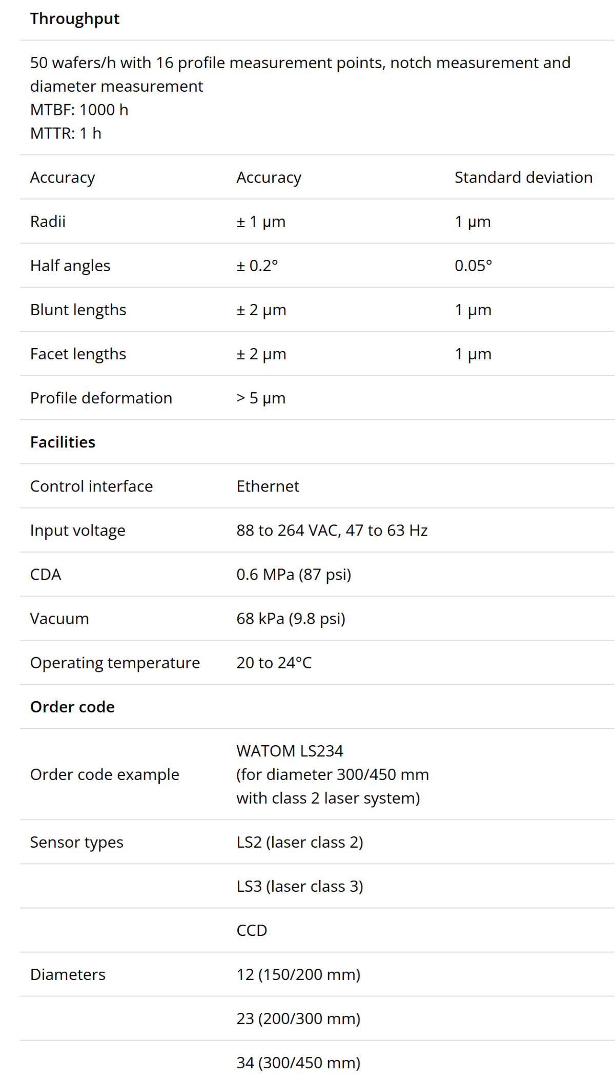

晶圓邊緣量測系統-極高精度
Wafer Edge Measurement-pinpoint precise 型號:WATOM LS
隨著半導體產業圖形尺寸持續微縮,對材料品質的要求也越來越嚴苛。為因應晶圓品質不斷提升的需求,KoCoS Optical Measurement 開發了 WATOM —— 一套用於晶圓邊緣與缺口輪廓量測的設備,開啟了高精度晶圓幾何量測的新時代。
-
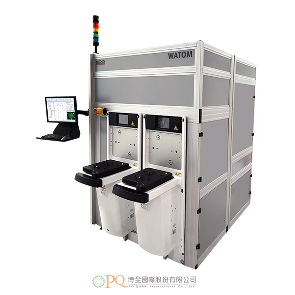
WATOM-晶圓邊緣的半導體量測技術
KoCoS 推出的 WATOM 晶圓邊緣量測系統,為邊緣研磨與拋光製程的品質保證與製程控制樹立了全球標竿,結合最高品質標準與頂級服務水準。
其專利雷射量測技術可在晶圓整個圓周的任意位置進行邊緣輪廓量測,甚至可深入量測缺口內部的輪廓。全球領先的晶圓製造商皆採用 WATOM 作為其最先進的晶圓邊緣幾何量測設備。
晶圓邊緣量測系統-極高精度
隨著半導體產業圖形尺寸持續微縮,對材料品質的要求也越來越嚴苛。為因應晶圓品質不斷提升的需求,KoCoS Optical Measurement 開發了 WATOM —— 一套用於晶圓邊緣與缺口輪廓量測的設備,開啟了高精度晶圓幾何量測的新時代。
WATOM LS 採用專利量測方法,利用光切式(Light Sectioning)感測器,以極高精度量測晶圓邊緣輪廓,並可涵蓋缺口內部的輪廓。系統透過 CMOS 相機拍攝由邊緣輪廓所產生的雷射線影像,再運用 KoCoS 所開發的數學演算法,精確計算並解析邊緣輪廓的各項特性。
WATOM 採用模組化設計,可與多種自動化解決方案整合,適用於現代半導體製程,無論是人工上片或自動化物料搬運系統(AMHS)皆可順利搭配。
-
-
WATOM - Semiconductor Metrology on the Edge
The wafer edge profiler WATOM from KoCoS sets the worldwide benchmark for the quality assurance and process control of edge grinding and polishing process combining the highest quality standards with top-class service.
The patent laser technology measures the edge profile not only on any point of the circumference even so inside the notch. Leading wafer manufacturer across the world use WATOM as their state-of–the art tool for geometrical measurement of wafer edge.
Wafer Edge Measurement - pinpoint precise
The use of smaller and smaller patterns in the semiconductor industry calls for increasingly advanced materials of extremely high quality. In response to the steady improvements in the quality of wafers, KoCoS Optical Measurement has developed WATOM, a wafer edge and notch profile measurement tool which heralds a new era of extremely precise wafer geometry measurement.
The patented measurement method of WATOM LS utilizes a lightsectioning sensor to measure the profile of the wafer edge with pinpoint precision, including the profile within the notch. Using a CMOS camera, pictures are taken of the laser line produced by the edge profile. A mathematical algorithm developed by KoCoS is then used to determine the edge profile characteristics.
The modular design of WATOM is prepared to be combined with various automation solutions for modern semiconductor manufacturing processes, whether individual wafers are loaded manually or an automated material handling system (AMHS) is in place. -