


-
 AstroNova
-
 AOiP
AOiP
-
 ADASH
ADASH
-
 Amptek
-
 Automatic Research
-
 AWSensors
-
 AARONIA AG
-
 BASI
BASI
-
 CALMET
-
 DV Power
-
 DANATRONICS
-
 Dioxide Materials
-
 ED & D
-
 ELVEFLOW
-
 ECH
ECH
-
 Elsys
Elsys
-
 EA Technology
-
 Enapter
-
 Electrothermal
-
 Enervac
-
 EL-CELL
-
 ENERGY SUPPORT
-
 FASTEC
-
 GMW
GMW
-
 Gaskatel
-
 GIUSSANI
-
 Globecore
-
 GRZ
GRZ
-
 HVPD
HVPD
-
 HIGH SENSE SOLUTIONSHTW
-
 HUBER
HUBER
-
 IVIUM
IVIUM
-
 Ida
Ida
-
 Instytut Fotonowy
-
 JGG
JGG
-
 Jacomex
-
 Jenway
-
 Kocos
Kocos
-
 KEHUA TECH
-
 micrux
-
 Metrel
-
 Microrad
-
 METERTEST
-
 ndb
ndb
-
 Norecs
-
 Novocontrol
-
 Neware
-
 OKOndt Group
-
 OZM
OZM
-
 Pine Research
-
 Pinflow
-
 Redoxme
-
 SATIR
SATIR
-
 Sonel
Sonel
-
 Serstech
-
 SDT
SDT
-
 SENSIA
-
 SIKA
SIKA
-
 SMC
SMC
-
 TANDELTA
-
 TENTECH
-
 Turnkey Instruments
-
 VacCoat
-
 Zurich Instruments
- AstroNova
- AOiP
- ADASH
- Amptek
- Automatic Research
- AWSensors
- AARONIA AG
- BASI
- CALMET
- DV Power
- DANATRONICS
- Dioxide Materials
- ED & D
- ELVEFLOW
- ECH
- Elsys
- EA Technology
- Enapter
- Electrothermal
- Enervac
- EL-CELL
- ENERGY SUPPORT
- FASTEC
- GMW
- Gaskatel
- GIUSSANI
- Globecore
- GRZ
- HVPD
- HIGH SENSE SOLUTIONSHTW
- HUBER
- IVIUM
- Ida
- Instytut Fotonowy
- JGG
- Jacomex
- Jenway
- Kocos
- KEHUA TECH
- micrux
- Metrel
- Microrad
- METERTEST
- ndb
- Norecs
- Novocontrol
- Neware
- OKOndt Group
- OZM
- Pine Research
- Pinflow
- Redoxme
- SATIR
- Sonel
- Serstech
- SDT
- SENSIA
- SIKA
- SMC
- TANDELTA
- TENTECH
- Turnkey Instruments
- VacCoat
- Zurich Instruments
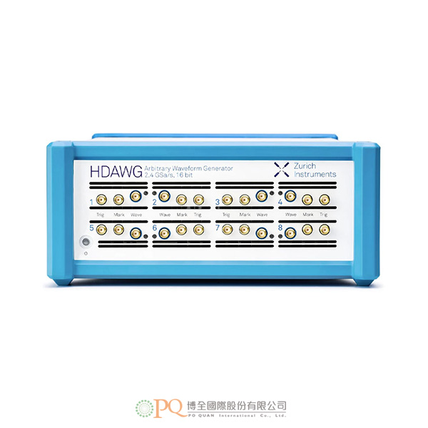

750 MHz 任意波形產生器
750 MHz Arbitrary Waveform Generator 型號:HDAWG- 2.4 GSa/s,16 位,頻寬750 MHz
- 最大輸出幅值5 V pp
- 最多可擴展至144 個輸出通道
- 觸發輸出延遲小於50 ns
- 可實現多頻率數位調製
- LabOne ® AWG 定序器和編譯器
-
簡介
Zurich Instruments 的多通道任意波形產生器HDAWG 擁有同類產品中最高的通道密度,其設計旨在實現高級的信號產生功能,頻寬高達750 MHz 。HDAWG 擁有4 或8 個直流耦合單端模擬輸出通道,輸出垂直分辨率為16 位。每個模擬輸出有兩個可切換模式,直接模式(最高頻寬和超低噪聲)和放大模式(最高輸出幅值為 5 V pp )。至多18 台HDAWG 可以通過我們的可編程量子系統控制器PQSC 實現時間同步。
LabOne提供了先進的編程理念,它結合了 AWG 的高性能、靈活性和函數產生器的易用性。使用LabOne 用戶界面(UI) 以及適用於LabVIEW™、.NET、MATLAB ®、C 和Python 的API,用戶可以輕鬆實現自動化測量以及快速整合HDAWG 至現有控制環境。應用
- 量子計算
- 雷達/雷射雷達
- 核磁共振譜 (NMR) 和電子順磁共振譜( EPR)
- 半導體器件測試
- 磁共振成像(MRI) 和電信應用中的多輸入多輸出(MIMO) 技術
特色
高級AWG 編程
LabOne UI 以一種直觀、輕鬆可讀的形式提供硬體控制,方便用戶快速掌握。在LabOne AWG 序列編程器中定義波形和序列後,LabOne AWG 編譯器會在最短的時間內將指令轉換為機器語言並將結果傳送到硬體。LabOne 定序功能支持具有動態變化延遲和條件分支點的迴路。
除Gaussian、Blackman、正弦等標準波形之外,LabOne 還包括複雜波形設計需要使用的所有重要數學和陣列編輯工具。用戶可輕鬆對波形進行相加、相乘、剪切和連接,還可以對波形進行分段整理。測量信號或在MATLAB 等工具中計算的波形只需通過拖放操作便可導入。
-
任意波形產生器
通道數1 4 (HDAWG4) 或8 (HDAWG8)
垂直分辨率
16 位
每個通道的波形存儲器
64 MSa;
500 MSa(使用 HDAWG-ME 選配件)定序器最大長度
8192 條指令
波形粒度
16 個樣本
最小波形長度
32 個樣本
定序器時鐘頻率
採樣率除以 8
定序器指令(播放)
播放波形(單通道或多通道),
播放波形片段(起始樣本索引和分段長度),
播放來自庫的波形(DIO 輸入狀態),中斷波形回放定序器指令(其他)
等待常量、等待觸發、設置/獲取觸發狀態、設置/獲取DIO 狀態、
整型變量運算(加、減、邏輯運算)、
更改振盪器頻率/相位(實時)、更改其他儀器設置(非實時)定序器控制結構
重複(1 到2 23 -1 或無窮大),條件分支(多分支)
波形信號輸出
接口類型SMA
輸出阻抗
50 Ω
輸出耦合
DC
輸出模式
放大輸出,直接輸出
輸出幅度範圍(50 Ω)
0.2 V pp到5.0 V pp(放大)
0.8 V pp(直接)輸出幅度精度
±(1% 幅度設置範圍+ 5 mVpp) (放大, 50 Ω)
輸出幅度分辨率
< 0.1 mV
偏置電壓
0.5 × 峰峰值電壓, 最大±1.25 V (放大, 50 Ω)
0 V (直接)偏置電壓精度
±(1% 幅度設置範圍+ 5 mV)
相位噪聲
< -135 dBc/Hz (放大, 1 V pp , 100 MHz, 偏移10 kHz)
< -148 dBc/Hz (放大, 1 V pp , 100 MHz, 偏移1 MHz)
< -135 dBc/Hz (直接, 0.5 V pp , 100 MHz, 偏移10 kHz)
< -148 dBc/Hz (直接, 0.5 V pp , 100 MHz, 偏移1 MHz)波形輸出週期抖動
3 ps RMS (方波, 150 MHz)
電壓噪聲
(> 200 kHz)35 nV/√Hz (放大, ±2.5 V 範圍, 高阻)
12 nV/√Hz (直接, 高阻)均方根(RMS) 電壓噪聲
(積分範圍: 100 Hz 到600 MHz)320 µVrms (放大, ±2.5 V range, 50 Ω)
100 µVrms (直接, 50 Ω)時域和頻域特性
輸出頻寬(-3dB, 校準sin(x)/x 滾降後) 0 - 300 MHz (放大, ±2.5 V 範圍)
0 - 750 MHz (直接)採樣率
100 MSa/s 至2.4 GSa/s
採樣率除法器
2 0 to 2 13
內部採樣時鐘分辨率
7 位
上升時間(20% 至80%)
450 ps (0.2 V , 放大, ±0.4 V 範圍)
800 ps (1 V, 放大, ±2.5 V 範圍)
1100 ps (5 V, 放大, ±2.5 V 範圍)
300 ps (0.8 V, 直接)
550 ps (1 V, 放大, ±1.5V 範圍)過衝
< 1%
觸發輸出延遲
< 50 ns (限於成對輸出信號1&2, 2&4, 5&6, 7&8 並使用時序指令playWaveDigTrigger)
< 180 ns (使用時序指令waitDigTrigger)通道間偏移
< 200 ps
偏移調節範圍
10 ns
時偏移節精度
< 10 ps (使用HDAWG-SKW 選配件)
< 0.42 ns or 1 個採樣時鐘週期(無HDAWG-SKW 選配件)標記和其他輸出
標記輸出 1 個/通道, SMA (前面板), 2 標記比特/波形
標記輸出阻抗
50 Ω
標記輸出上升/下降時間
300 ps (20/80%)
標記輸出週期抖動
60 ps 峰峰值(方波, 100 MHz)
標記輸出偏移調節
範圍:-23 至30 ns (最高采樣率)
分辨率:~10 ps (最高采樣率, 取決於設置)採樣時鐘輸出
後面板SMA
採樣時鐘輸出幅度
0.8 V pp (2.4 GHz, 50 Ω)
2.0 V pp (1.0 GHz, 50 Ω)參考時鐘輸出
後面板SMA
參考時鐘輸出阻抗
50 Ω, AC 耦合
參考時鐘輸出幅度
1 V pp (100 MHz, 50 Ω)
參考時鐘輸出頻率
100 MHz (內部參考模式)
10 / 100 MHz (外部參考模式)參考時鐘輸出抖動
260 fs RMS, 由相位噪聲積分導出(12 kHz 至200 MHz 頻率偏移範圍)
輸入
觸發輸入 每個通道1 路輸入,前面板配有SMA 接口
觸發輸入阻抗
50 /1 kΩ
觸發輸入幅值範圍
± 5 V (50 Ω)
± 10 V (1 kΩ)觸發輸入閾值範圍
± 5 V (50 Ω)
± 10 V (1 kΩ)觸發輸入閾值分辨率
< 0.4 mV
觸發輸入閾值遲滯
> 60 mV
觸發輸入最小脈衝寬度
5 ns
觸發輸入最高運行頻率
300 MHz
採樣時鐘輸入
後面板SMA
參考時鐘輸入
後面板SMA
參考時鐘輸入阻抗
50 Ω, AC 耦合
參考時鐘輸入頻率
10 / 100 MHz
參考時鐘輸入幅度
-4 dBm 至+13 dBm
振盪器和時鐘
內部時鐘類型 TXCO
內部時鍾老化
±0.8 ppm/年
內部時鐘短期穩定度
0.0001 ppm (1 s)
內部時鐘初始精度
±1 ppm
內部時鐘溫度穩定度
±0...3 ppm (–20°C 至 +70°C)
內部時鐘相位噪聲
-105 dBc/Hz (偏移100 Hz)
-125 dBc/Hz (偏移1 kHz)最大額定值
波形損傷閾值 -1.2 V / +1.2 V (直接)
-6 V / +6 V (放大)標記損傷閾值
-0.7 / +4 V
觸發損傷閾值
-11 V / +11 V (1 kΩ 輸入阻抗)
-6 V / +6 V (50 Ω 輸入阻抗)參考時鐘輸入損傷閾值
-4 V / +4 V (DC)
+13.5 dBm (AC, DC 偏置0 V)參考時鐘輸出損傷閾值
-4 V / +4 V (DC)
採樣時鐘輸入損傷閾值
-4 V / +4 V (DC)
+13.5 dBm (AC, DC 偏置0 V)採樣時鐘輸出損傷閾值
-4 V / +4 V (DC)
MDS 輸入/輸出損傷閾值
-0.7 / +4 V
DIO 輸入/輸出損傷閾值
-0.7 / +4 V (默認設置3.3 V CMOS/TTL)
連接接口和其他
數位輸入輸出(DIO) VHDCI 68 針母頭,
32 位, 配置為輸入或輸出, 3.3 V TTL主機連接接口
LAN/Ethernet, 1 Gbit/s
USB 3.0, 5 Gbit/s主機內存要求
4 GB+
主機處理器
相容SSE2 指令。
如: AMD K8 (Athlon 64, Sempron 64, Turion 64, etc.),
AMD Phenom, Intel Pentium 4, Xeon, Celeron, Celeron D,
Pentium M, Celeron M, Core, Core 2, Core i5, Core i7, Core i3, Atom操作系統
詳見 LabOne 相容性
物理特性
尺寸 43.0 × 23.2 × 10.2 cm
16.9 × 9.2 × 4.0 英寸,適用於19 英寸機架重量
4.6 kg;10.2 磅
交流電源線
100-240 V (±10%),50/60 Hz
工作溫度
+5 °C 到+40 °C
工作環境
IEC61010,室內工作,安裝類別II,污染等級 2
工作海拔
最高2000 米
-
Introduction
The Zurich Instruments HDAWG multi-channel Arbitrary Waveform Generator has the highest channel density available in its class, and is designed for advanced signal generation up to 750 MHz bandwidth. The HDAWG comes with either 4 or 8 DC-coupled, single-ended analog output channels with 16-bit vertical resolution. Output switching is supported between a direct mode with maximized bandwidth and superior noise performance and an amplified mode that boosts the signal amplitude to a maximum of 5 Vpp. Temporal synchronization of up to 18 HDAWGs is supported through the PQSC.LabOne provides a state-of-the-art programming concept that combines the performance and flexibility of an arbitrary waveform generator with the accessibility of a function generator. The LabOne user interface and a choice of APIs for Python, C, MATLAB®, LabVIEW™ and .NET enable measurement automation and fast integration into an existing control environment.
Applications
- Quantum computing
- Radar / Lidar
- NMR and EPR spectroscopy
- Semiconductor testing
- MIMO techniques in MRI and telecommunication
Highlights
High-level AWG programming
Once the waveforms and sequences are defined in the LabOne AWG Sequencer, the LabOne AWG Compiler translates the instructions into machine language and transfers the result to the hardware in a minimum amount of time. LabOne sequencing supports loops with dynamically varying delay and conditional branching points.In addition to the standard waveforms (such as Gaussian, Blackman, sinc, etc.), LabOne contains all essential math and array editing tools required for complex waveform design. It is possible to add, multiply, cut, and concatenate waveforms as well as to organize them in segments. Importing measured signals or waveforms calculated with MATLAB®, for instance, amounts to a simple drag-and-drop action.
-
Arbitrary waveform generator
Channels 4 (HDAWG4 model)
8 (HDAWG8 model)Vertical resolution 16 bits Waveform memory per channel 64 MSa;
500 MSa (with HDAWG-ME option)Sequence length 8,192 Waveform granularity 16 samples Minimum waveform length 32 samples Sequencer clock frequency Sampling rate divided by 8 Sequencer instructions (playback) Play waveform (single or multi-channel),
play waveform segment (start sample index and segment length),
play waveform from the library (DIO input state), interrupt waveform playbackSequencer instructions (other) Wait constant, wait for trigger, set/get trigger state, set/get DIO state,
integer variable operations (add, subtract, logical operations),
change oscillator frequency/phase (real-time), change other
instrument setting (non real-time)Sequencer control structures Repeat (1 to 223-1 or infinite), conditional branch (multi-branch) Wave Signal Output
Connector type SMA (front panel, single-ended) Output impedance 50 Ω Output coupling DC Output modes Amplified, direct Output range ±0.1 V to ±2.5 V (amplified, into 50 Ω)
±0.4 V (direct)Output level accuracy ±(1% of setting + 5 mVpp) (amplified, into 50 Ω) Output level resolution < 0.1 mV Offset voltage 0.5 × peak voltage, max. ±1.25 V (amplified, into 50 Ω)
0 V (direct)Offset voltage accuracy ±(1% of setting + 5 mV) Phase noise < -135 dBc/Hz (amplified, 1 Vpp, 100 MHz, offset 10 kHz)
< -148 dBc/Hz (amplified, 1 Vpp, 100 MHz, offset 1 MHz)
< -135 dBc/Hz (direct, 0.5 Vpp, 100 MHz, offset 10 kHz)
< -148 dBc/Hz (direct, 0.5 Vpp, 100 MHz, offset 1 MHz)Wave output period jitter 3 ps RMS (square wave, 150 MHz) Voltage noise
above 200 kHz35 nV/√Hz (amplified, ±2.5 V range, into high impedance)
12 nV/√Hz (direct, into high impedance)RMS voltage noise
(integrated from 100 Hz to 600 MHz)320 µVrms (amplified, ±2.5 V range, into 50 Ω)
100 µVrms (direct, into 50 Ω)Time- and frequency-domain characteristics
Wave output bandwidth (-3dB, after correcting for sin(x)/x roll-off) 0 - 300 MHz (amplified, ±2.5 V range)
0 - 750 MHz (direct)Sampling rate 100 MSa/s to 2.4 GSa/s Sampling rate divider 20 to 213 Internal sampling clock resolution 7 digits Rise time (20% to 80%) 450 ps (0.2 V step, amplified, ±0.4 V range)
800 ps (1 V step, amplified, ±2.5 V range)
1100 ps (5 V step, amplified, ±2.5 V range)
300 ps (0.8 V step, direct)
550 ps (1 V step, amplified, ±1.5V range)Overshoot < 1% Trigger delay to output < 50 ns (within one channel pair 1&2, 2&4, 5&6, 7&8 using playWaveDigTrigger sequencer instruction)
< 180 ns (using waitDigTrigger sequencer instruction)Skew between channels < 200 ps Skew control range 10 ns Skew control resolution <10 ps (with HDAWG-SKW option)
<0.42 ns or 1 sample clock period (without HDAWG-SKW option)Marker and other outputs
Marker outputs 1 per channel, SMA (front panel), 2 marker bits per waveform Marker output impedance 50 Ω Marker output rise/fall time 300 ps (20/80%) Marker output period jitter 60 ps p-p (square wave, 100 MHz) Marker output skew control -23...30 ns (range, at max. sampling rate)
~10 ps (resolution, at max. sampling rate, depends on absolute setting)Sampling clock output SMA on back panel Sampling clock output amplitude 0.8 Vpp (2.4 GHz into 50 Ω)
2.0 Vpp (1.0 GHz into 50 Ω)Reference clock output SMA on back panel Reference clock output impedance 50 Ω, AC coupled Reference clock output amplitude 1 Vpp (100 MHz into 50 Ω) Reference clock output frequency 100 MHz (internal reference mode)
10 / 100 MHz (external reference mode)Reference clock output jitter 260 fs RMS, derived from integrated phase noise measurement (12 kHz to 200 MHz offset frequency) Inputs
Trigger inputs 1 per channel, SMA (front panel) Trigger input impedance 50 Ω / 1 kΩ Trigger input voltage range ±5 V (50 Ω)
±10 V (1 kΩ)Trigger input threshold range ±5 V (50 Ω)
±10 V (1 kΩ)Trigger input threshold resolution < 0.4 mV Trigger input threshold hysteresis > 60 mV Trigger input min. pulse width 5 ns Trigger input max. operating frequency 300 MHz Sampling clock input SMA (back panel) Reference clock input SMA (back panel) Reference clock input impedance 50 Ω, AC coupled Reference clock input frequency 10 / 100 MHz Reference clock input amplitude -4 dBm to +13 dBm Oscillators and clocks
Internal clock type TXCO Internal clock aging ±0.8 ppm/year Internal clock short-term stability 0.0001 ppm (1 s) Internal clock initial accuracy ±1 ppm Internal clock temperature stability ±0..3 ppm (–20°C to +70°C) Internal clock phase noise -105 dBc/Hz (offset 100 Hz)
-125 dBc/Hz (offset 1 kHz)Maximum ratings
Damage threshold Wave -1.2 V / +1.2 V (direct)
-6 V / +6 V (amplified)Damage threshold Mark -0.7 / +4 V Damage threshold Trig -11 V / +11 V (1 kΩ input impedance)
-6 V / +6 V (50 Ω input impedance)Damage threshold Reference Clk In -4 V / +4 V (DC)
+13.5 dBm (AC, with DC offset 0 V)Damage threshold Reference Clk Out -4 V / +4 V (DC) Damage threshold Sample Clk In -4 V / +4 V (DC)
+13.5 dBm (AC, with DC offset 0 V)Damage threshold Sample Clk Out -4 V / +4 V (DC) Damage threshold MDS In/Out -0.7 / +4 V Damage threshold DIO In/Out -0.7 / +4 V (default configuration 3.3 V CMOS/TTL) Connectivity and others
Digital IO (DIO) VHDCI 68 pin female connector,
32-bit, configurable as input or output, 3.3 V TTLHost connection LAN/Ethernet, 1 Gbit/s
USB 3.0, 5 Gbit/sPC memory requirements 4 GB+ PC CPU requirements Compatibility with SSE2 instruction set required.
Examples: AMD K8 (Athlon 64, Sempron 64, Turion 64, etc.),
AMD Phenom, Intel Pentium 4, Xeon, Celeron, Celeron D,
Pentium M, Celeron M, Core, Core 2, Core i5, Core i7, Core i3, AtomOperating system See LabOne Compatibility General
Dimensions 43.0 × 23.2 × 10.2 cm
16.9 × 9.2 × 4.0 inch, suited for 19 inch rackWeight 4.6 kg; 10.2 lbs Power supply AC line 100−240 V (±10%), 50/60 Hz Operating temperature +5 °C to +40 °C Operating environment IEC61010, indoor location, installation category II, pollution degree 2 Operating altitude Up to 2000 m